A new radiation-resistant semiconductor from Hiroshima University and Phenitec Semiconductor could address one of Fukushima Daiichi’s most stubborn technical limits: keeping electronics and wireless-linked systems working in places where conventional silicon fails. The prototype, announced by Hiroshima University on April 24, 2025, is built on silicon carbide and is designed to operate at up to 500°C while tolerating intense radiation, a combination directly relevant to decommissioning work inside and around the damaged reactors.
That matters because Fukushima’s cleanup still depends on remote inspection, robotics and data collection in areas too dangerous for people to enter. Tokyo Electric Power Company, or TEPCO, and its partners have repeatedly relied on robots, drones and remote-controlled systems to inspect reactor interiors, measure radiation and retrieve debris samples, yet high radiation, rubble and communications constraints have slowed progress for years. AP reported that full-scale removal of melted fuel debris has been pushed back to 2037 or later, underscoring how every improvement in durable electronics can affect the project timeline.
💡
The core finding is simple:
Hiroshima University said its first prototype radiation-resistant chip was successfully produced at a mass-production facility and can function at 500°C, a threshold far beyond ordinary consumer-grade electronics, on April 24, 2025.
500°C Operation Targets Fukushima’s Harshest Zones
The chip is not being marketed as a consumer Wi-Fi component. Its significance is more foundational. Hiroshima University described it as a step toward establishing a silicon carbide, or SiC, integrated-circuit foundry, while Asahi Shimbun reported that the device was created specifically for extreme heat and radiation environments, including nuclear decommissioning. Professor Shinichiro Kuroki, who led the project, said one of the most urgent tasks is developing chips that can support work at Fukushima Daiichi.
Silicon carbide is important because it belongs to a class of wide-bandgap semiconductors known for higher thermal tolerance and stronger radiation hardness than standard silicon. That does not automatically solve every communications problem at Fukushima, but it can make radios, sensor nodes, control circuits and edge devices more likely to survive where existing electronics degrade or fail. Research literature also supports SiC’s suitability for harsh environments, including radiation-heavy applications.
Key Data Behind the Fukushima Communications Problem
| Metric | Latest verified detail | Why it matters |
|---|---|---|
| Chip operating temperature | Up to 500°C | Supports electronics in extreme heat zones |
| Prototype announcement | April 24, 2025 | Marks first disclosed production milestone |
| Melted fuel debris at Fukushima | At least 880 tons | Shows scale of long-term remote operations |
| Full-scale debris removal | Delayed to 2037 or later | Extends need for durable robotics and sensors |
Source: Hiroshima University, AP | accessed March 24, 2026
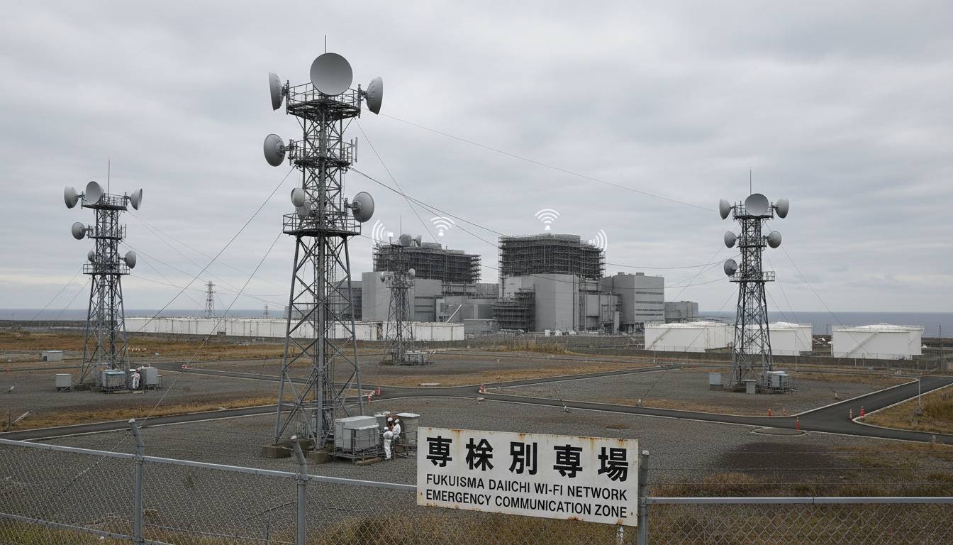
Why Radiation and Thick Structures Disrupt Wireless Systems
The “Wi-Fi problem” at Fukushima is really a broader communications problem. Inside damaged reactor buildings, signals must pass through reinforced concrete, steel, water, debris and highly contaminated zones. Wired systems can be more reliable, but cables limit mobility and can snag on rubble. Wireless systems offer flexibility, yet they depend on electronics that must keep functioning under radiation stress. Wired reported that some Fukushima robots had to drag long electric cables because water and thick walls would defeat wireless signals.
TEPCO’s own post-accident review shows how vulnerable plant communications were after the 2011 disaster. The station blackout rendered in-house communication tools such as PHS handsets and fixed-line phones inoperable, forcing emergency reliance on transceivers and ad hoc measures. That history matters because Fukushima’s decommissioning is still, in part, a communications engineering challenge: operators need dependable links between sensors, robots and control rooms in a site that was never designed for post-meltdown remote work.
Fukushima Decommissioning and Remote-Tech Timeline
March 11, 2011: Earthquake and tsunami trigger station blackout and reactor meltdowns at Fukushima Daiichi, disabling normal in-house communications.
2022: Boston Dynamics says Spot begins use at Fukushima Daiichi for data collection, video capture, radiation measurement and debris sampling support.
November 2024: A robot retrieves a tiny melted fuel sample, a key technical milestone for future cleanup planning.
April 24, 2025: Hiroshima University announces a first prototype of a radiation-resistant SiC chip operating at 500°C.
2037 or later: AP reports full-scale melted fuel debris removal is delayed beyond earlier targets.
How a SiC Chip Could Improve Robot Links and Sensor Networks
The most realistic near-term impact is not household Wi-Fi inside the plant. It is tougher electronics for the systems that make remote work possible: wireless repeaters, radiation-tolerant sensors, onboard robot controls, camera modules and communication subsystems placed closer to hazardous areas. If those components survive longer, operators can reduce downtime, gather more data per mission and potentially place relay points in zones that are now too punishing for standard hardware. That is an inference from the chip’s published characteristics and Fukushima’s documented operating constraints.
There is already evidence that decommissioning progress depends on specialized machines. AP said the first sample retrieval in November 2024 was a crucial step toward developing technology and robots for larger-scale cleanup. Boston Dynamics separately notes that crews use robots to collect data, shoot video, measure dose rates and gather debris samples. In that context, a more durable semiconductor platform could matter less as a standalone product and more as an enabling layer for the next generation of inspection and communications hardware.
Conventional Silicon vs Silicon Carbide in Fukushima-Type Conditions
| Characteristic | Conventional silicon | Silicon carbide |
|---|---|---|
| High-temperature tolerance | More limited | Higher tolerance |
| Radiation resilience | Lower in harsh environments | Better suited for harsh environments |
| Use case at Fukushima | Shorter life in extreme zones | Potential fit for sensors, controls, communications |
Source: Hiroshima University, Asahi Shimbun, academic SiC studies | accessed March 24, 2026
What 2037 Delays Mean for the Chip’s Commercial Relevance
Fukushima’s cleanup is measured in decades, not quarters. AP reported in 2024 that full-scale removal of melted fuel debris would be delayed until 2037 or later, while the broader decommissioning target remains 2051. That long horizon creates a sustained need for components that can survive radiation, heat and limited maintenance access.
That does not mean the Hiroshima-Phenitec chip is already deployed at Fukushima. Publicly available reporting and the university release describe a prototype and a manufacturing milestone, not a field installation. The verified story is narrower but still significant: Japan now has a disclosed prototype of a mass-production-fabricated SiC chip aimed at environments that include Fukushima decommissioning. In a cleanup effort where robots have been delayed by equipment glitches, navigation problems and harsh conditions, that is a meaningful engineering development.
Frequently Asked Questions
Frequently Asked Questions
What is the chip made of?
The prototype uses silicon carbide, or SiC, according to Hiroshima University and Asahi Shimbun. SiC is a wide-bandgap semiconductor known for operating in higher heat and harsher radiation environments than standard silicon. Hiroshima University disclosed the prototype on April 24, 2025.
Does the chip literally fix Wi-Fi at Fukushima Daiichi?
Not directly, based on public reporting. The verified claim is that it is a radiation-resistant, high-temperature chip relevant to decommissioning. Its likely value is enabling tougher communications and sensor electronics in areas where ordinary components fail, rather than acting as a standalone Wi-Fi fix.
Why is wireless communication difficult at the plant?
Fukushima combines thick concrete and steel structures, debris, water, and intense radiation. Wired reported that thick walls and water can defeat wireless signals for some robots, while TEPCO’s records show the 2011 station blackout disabled normal in-house communications, forcing emergency alternatives.
How far along is Fukushima’s cleanup?
The cleanup remains in an early technical phase relative to its full scope. AP reported that Fukushima contains at least 880 tons of melted fuel debris and that full-scale removal has been delayed to 2037 or later, with overall decommissioning targeted for 2051.
Has the chip been installed at Fukushima yet?
No public source reviewed here confirms deployment at the plant. Hiroshima University describes a successful prototype produced at a mass-production facility, which is an important development step, but not the same as field use inside Fukushima Daiichi.
Disclaimer: This article is for informational purposes only. Information may have changed since publication. Always verify information independently and consult qualified professionals for specific advice.
View 0 comments